8Layer Immersion Gold Finished Multilayer Printed Circuit Prototype
PCB Board
What is a Multilayer PCB?
A Multilayer PCB is a printed circuit board that has more than 2
layers, unlike a
double sided PCB or a 2 layer PCB board, which only has two conductive layers of
material. All multilayer PCB’s must have at least three layers of
conductive material.
A Multilayer PCB is much more complex than a double-sided PCB
design and can have any number of layers - choose from 4 layer PCBs
to 6 layer PCBs, 8 layers or even up to 64 layers. Multilayer PCB’s
are laminated and glued together with layers of heat protection
insulation between them.
What is the purpose of a multilayer PCB?
Multilayer boards provide both high capacity and speed in a smaller
footprint by their innate electrical properties. Connectors that
are required for multiple separate PCBs are reduced or eliminated,
simplifying construction and further reducing weight.
Multilayer PCB Board Thickness
Multilayer board thickness is 370 mil and the finished copper
weight inner layer 15 oz/ outer layer 15oz. The line width & space
of a multilayer PCB is a minimum 3mil/3mi and a minimum drill size
cnc 4 mil. The minimum drill size laser drill of our multilayer
PCBs is 3 mil, with an aspect ratio of 18:01 and a maximum board
size of 43”x26”. The minimum core thickness for Pure's multilayer
PCBs is 2mil and the impedance control tolerance +/- 5%.
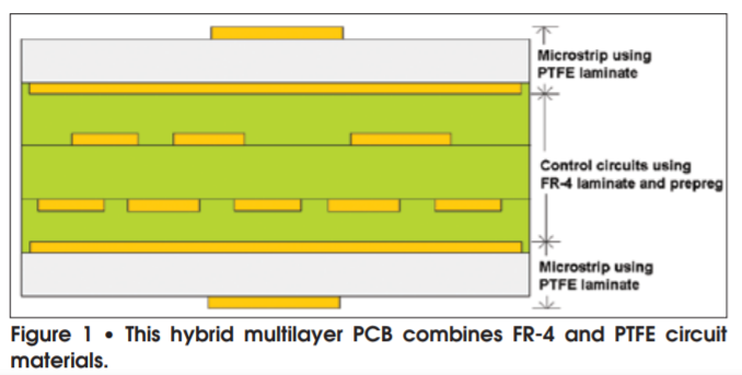
Hybrid multilayer PCBs often make use of circuit materials with
very different values of dielectric constant (Dk). For example,
some multilayer antenna circuits may consist of a low-Dk circuit
material as the outside layer for radiating elements, a moderate-Dk
circuit material internally for a stripline antenna feed line, and
a high-Dk material for an internal layer for filter circuitry. The
different Dk materials are often based on different resin systems.
The outer, low-Dk layer may be PTFE material while the inner,
moderateDk circuit layer is formed on a ceramic-filled
hydrocarbon-based laminate. The bonding materials could be based on
either type of material, although hydrocarbonbased bonding
materials are more often used for their ease of circuit
fabrication.
2 . Specifications:
| Name | 8Layer main board / immersion gold |
| Number of Layers | 8 |
| Quality Grade | IPC 6012 Class 2,IPC 6012 Class 3 |
| Material | IT180A + Rogers4350B + Copper Block |
| Thickness | 2.0mm |
| Min Track/Spacing | 100um/100um |
| Min drill Size | 0.2mm |
| Solder Mask | Green |
| Silkscreen | White |
| Surface Finish | Immersion gold |
| Finished Copper | 1OZ |
| Aspect ratio | 8:1 |
3. Product application
Printed circuit boards (PCBs) with characteristic impedance control
are widely used in high frequency circuit. PCB's that mixed high
frequency material can reduce signal loss at high frequencies and
meet the development needs of communication technology.
It is mainly used in the infrastructure field of transmission cores
including WDM/OTN end-to-end intelligent optical transmission
platform, MSTP/multi-service transmission platform, microwave
fusion transmission radio frequency, data communication system
platform, and other information communication industries.


